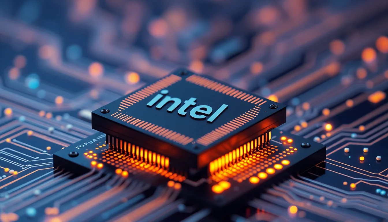
Advanced chip packaging has moved from a back-end manufacturing detail to a strategic choke point in AI infrastructure. That shift matters because the limiting factor in AI hardware is no longer just how many transistors a fab can print on a die. It is increasingly how many dies can be stitched together, how quickly they can talk to one another, how much power can be pushed through the assembly, and how much heat the package can remove before performance drops or yield collapses.
That is the opening Intel is trying to exploit. In the coverage this week, Wired described Intel’s “ridiculously nerdy” packaging bet as a way to ride the AI boom without waiting for a single breakthrough accelerator or process node. Ars Technica framed the same move more plainly: Intel is going all in on advanced chip packaging. The shared implication is that Intel does not need to win every transistor-density headline if it can become indispensable in the layer that makes high-end AI silicon usable at scale.
That layer is getting more valuable because single-die scaling is running into practical limits. AI accelerators increasingly rely on multi-die integration: one compute tile, one I/O tile, maybe high-bandwidth memory, all packed into a system that behaves like a single product. The packaging technology is what determines whether those dies can be linked with enough interconnect density to keep the tensor engines fed. In plain terms, if the links between dies are too slow or too sparse, the accelerator spends its time waiting instead of computing. If the power delivery network is sloppy, the chip cannot sustain its target clocks under load. If thermal paths are weak, the package throttles long before the silicon has exhausted its theoretical throughput.
This is why packaging is no longer just assembly. It is part of the architecture.
For AI silicon, the practical gains are tangible. A tighter package can shorten the electrical distance between compute and memory, which reduces latency and helps keep bandwidth-hungry workloads from stalling. Better thermal design can allow a larger aggregate power envelope without turning the module into a reliability problem. More sophisticated package layouts can also improve manufacturability by letting designers combine dies that are easier to yield separately instead of forcing everything onto one monolithic slab. That matters in AI because the market is now rewarding systems that can be delivered in volume, not just demonstrated in a lab.
Intel is making this bet now because the demand profile has changed. AI customers want faster product cycles, more heterogeneous designs, and enough supply to outfit hyperscale deployments rather than boutique pilot runs. That pushes value toward the companies that can integrate compute, memory, power delivery, and cooling into a repeatable product. Intel is signaling that it wants packaging to be one of its differentiators in exactly that moment, not as an afterthought to its foundry ambitions but as part of the product stack it can sell into the AI buildout.
The market comparison is telling. NVIDIA still dominates the economics of AI accelerators, but it is not primarily a packaging company; its leverage comes from silicon, software, and system-level integration. TSMC, by contrast, already sits at the center of advanced manufacturing and packaging ecosystems, with the scale and customer base to turn packaging capacity into a business line rather than a rescue mission. Amkor and other OSAT players have spent years building the assembly and test infrastructure that advanced packages demand. Intel’s claim is that it can combine design, foundry, and packaging more tightly than those rivals. Its weakness is obvious: it does not yet command the same trust, scale, or execution consistency that TSMC and the best-in-class packaging specialists already have.
That is the real strategic tension. Intel is not simply saying advanced packaging is important. It is betting that owning enough of this layer can change its market position in AI from follower to necessary partner. If customers need complex multi-die packages, Intel wants to be the company that can design, manufacture, and assemble them in one stack. If that works, the upside is not just better products; it is more control over the infrastructure economics around them.
But packaging is also where semiconductor promises go to die in silence. It is capital-intensive, yield-sensitive, and unforgiving at volume. A package that looks impressive in a demo can become expensive fast if interconnects fail, thermal margins are too tight, or supply-chain coordination breaks under real deployment schedules. Intel’s execution gap over the past several years is part of why investors and customers may still be cautious: advanced packaging requires disciplined manufacturing, not just a good slide deck. The company has to prove it can deliver repeatability, not one-off technical showcase parts.
What would success look like? Not a press release about packaging in the abstract, but Intel hardware appearing in AI systems that matter to hyperscalers, model builders, and infrastructure teams buying at scale. Watch for concrete evidence: named packaging methods tied to specific products, capacity expansion that suggests Intel can support volume rather than prototypes, and external customer wins that indicate the ecosystem trusts its assembly and integration stack. If those pieces start landing together, packaging could become more than a technical competency. It could become a procurement advantage.
For technical buyers, that is the real implication. The next round of AI infrastructure decisions will not be made on transistor counts alone. They will hinge on who can deliver dense, cool, power-efficient packages that keep multi-die systems stable in production. If Intel can own that layer, it may not have to win every chip war to profit from the market that chips are making possible.